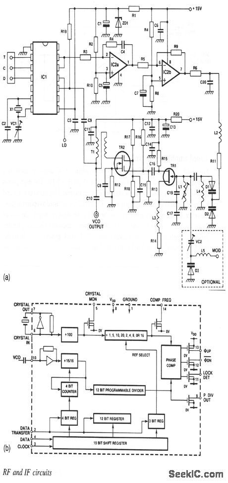
Frequency synthesizer Circuit Diagram
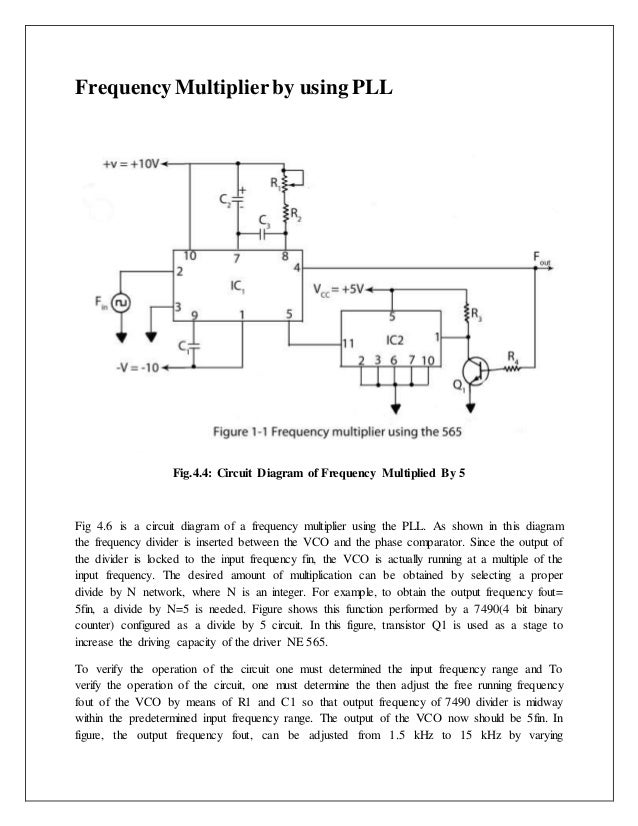
Frequency synthesizer Circuit Diagram The Fig. 2.130 shows the Frequency Synthesizer Block Diagram. It is similar to frequency multiplier circuit except that divided by M network is added at the input of phase lock loop . The frequency of the crystal-controlled oscillator is divided by an integer factor M by divider network to produce a frequency f osc /M, where f osc is the The actual design is best done with the computer program. A more complex filter as an application is shown in Figure 4. Fig. 4 — Phase/frequency comparator and loop for the 72 to 92 MHz frequency synthesizer. A detailed overview on how to design a synthesizer is found in the book, Microwave and Wireless Synthesizers: Theory and Design, a reference frequency fref, the division ratios of N and R, and the frequency fmix, applied to the mixer to down-convert the signal; the resulting output frequency, f out, will be out fref fmix R N f + = ⋅ Equ. 4 The main benefit of this method is the improved noise performance due to the reduced division in the loop. Loop Filter Design
the design of a frequency synthesizer in a transceiver environment, from the mapping of standard-specifications to its integrated circuit implementation in a CMOS technology. The results show that careful system level planning leads to high-performance realizations of the synthesizer. A strategy of using different supply voltages to enhance

PDF How to Design RF Circuits Circuit Diagram
A frequency synthesizer uses phase-locked loop (PLL) to generate output frequencies over a wide range. The typical range is from 1 MHz to 160 MHz. Fig: Block diagram of a frequency synthesizer. As illustrated in the block diagram above, the key components of the frequency synthesizer are: Crystal oscillator; Phase detector; Low-pass filter The RF frequency synthesizer design involves the integration of a Phase-Locked Loop (PLL) and a Voltage-Controlled Oscillator (VCO) to generate stable and tunable radio frequency signals. The synthesizer includes a control interface for user adjustments. RF frequency synthesizers are the cornerstone of modern communication systems, ensuring
High Speed Communication Circuits and Systems Lecture 18 Design and Simulation of Frequency Synthesizers Michael H. Perrott April 9, 2004 M.H. Perrott Outline Closed-Loop Design of Frequency Synthesizers-Introduction-Background on Classical Open Loop Design Approach-Closed Loop Design Approach-Example and Verification-Conclusion 2:00 - 3:30 RF front-end design - LNA, mixer 4:00 - 5:30 Frequency synthesizer design I (PLL) T d J l 22 2008Tuesday, July 22, 2008 9:00 - 10:30 Frequency synthesizer design II (VCO) 11:00 - 12:30 RFIC design for wireless communications 2:00 - 3:30 Analog and mixed signal testing Frequency synthesizer design I (PLL), FDAI, 2008 2 The synthesizer that we will be designing was extremely common back in the day. It's known as a 1V/Octave synthesizer. This means that for every 1V increase on the input, the output frequency will go up by one octave (i.e., by a factor of 2). Now for this module to work correctly, it needs an exponential converter on the input.